
Introduction to HDI PCB Technology

Today’s world is filled with high technology products, from advanced smartphones to powerful medical devices and ultra-reliable automotive systems. At the heart of all these innovations is the HDI PCB—High Density Interconnect Printed Circuit Board. Due to the ever-increasing wiring density per unit area, traditional printed circuit boards simply cannot keep pace with the demands for miniaturization and high performance.
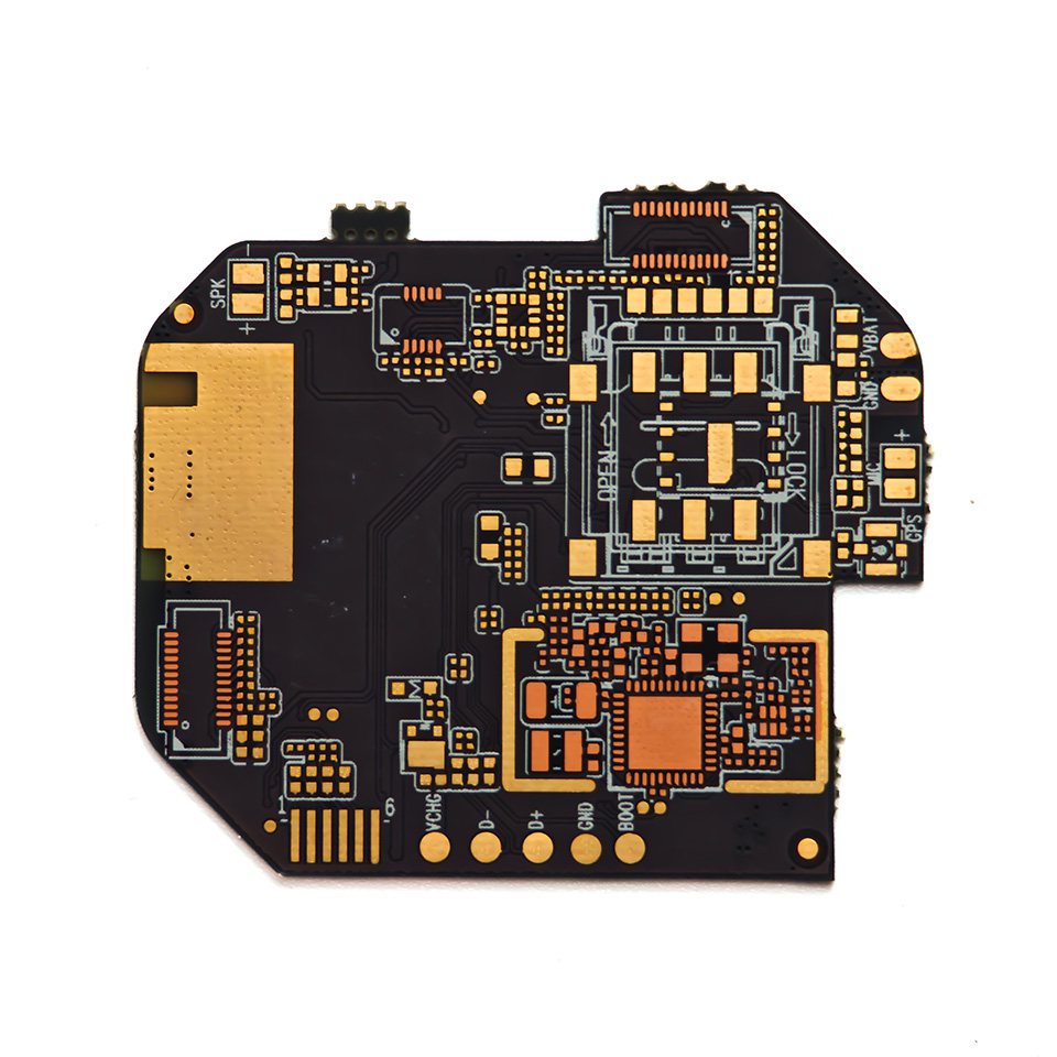
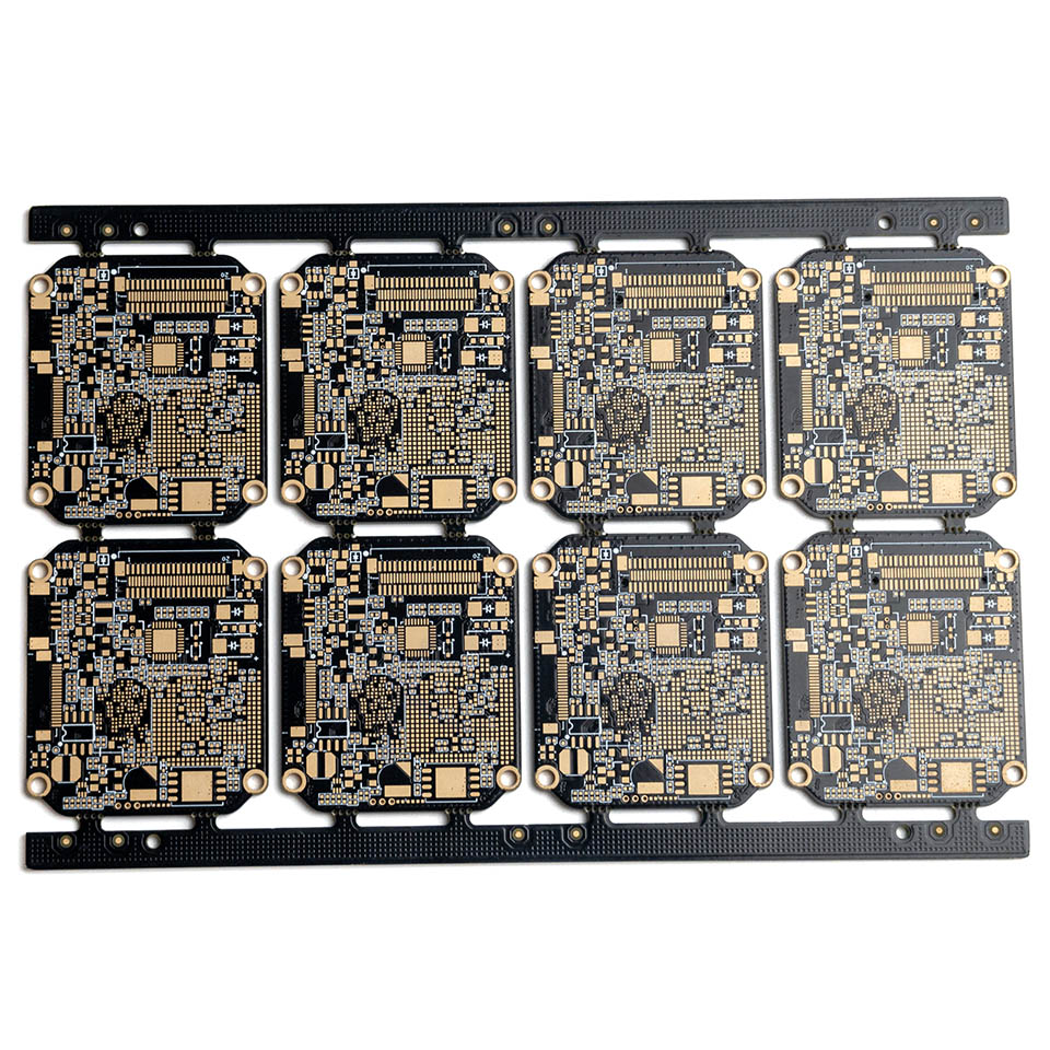
Consumer electronic products are becoming increasingly compact. These products need to integrate richer functionalities within limited space. High-Density Interconnect (HDI) printed circuit boards have thus become the standard choice in the field of electronic manufacturing. Such circuit boards are designed using advanced microvia technology and manufactured through precise processes. Within a unit area, these boards can accommodate more circuits. Their wiring density significantly exceeds that of traditional standard circuit boards. This characteristic makes them a crucial support for modern electronic manufacturing.
What Is an HDI PCB? High Density Interconnect Essentials

HDI PCBs—short for High Density Interconnect Printed Circuit Boards—stand apart for their ability to deliver far higher connection pad density, using microvias, blind vias, buried vias, and advanced PCB stack-up techniques. An HDI PCB stack-up achieves more routing layers and interconnects in the same or smaller area than traditional multi-layer PCBs.
Key Differences: HDI vs. Standard PCB
| Feature | HDI PCB | Standard PCB |
| Connection/Pad Density | Very high wiring density per unit area | Limited by mechanical vias |
| Microvias | Laser-drilled microvias | Mechanically drilled only |
| Blind/Buried Vias | Essential in HDI stack-ups | Rare or impossible |
| Layer Count Efficiency | Fewer PCBs needed for same circuitry | More or thicker layers |
| Signal Speed & Integrity | Enhanced with short paths | Lower, more EMI |
| Applications | Advanced, high-technology products | Commodity and legacy |
LHD TECH’S Key Features and Stack-Ups for High Density HDI PCBs

A successful HDI circuit board leverages a mix of technical strategies to boost circuit board density, signal integrity, and manufacturability:
- Microvias: Tiny, laser-drilled holes in a PCB that connect only adjacent layers, drastically increasing possible wiring density and making the unique layer stack-ups of HDI possible.
- Blind and Buried Vias:Specialized vias in PCBs, where a blind via connects an outer layer to an inner layer without passing through the entire board, and a buried via connects inner layers only. These are essential for dense routing close to fine-pitch components.
- Sequential Lamination Process:Multiple cycles of layer addition, drilling, and copper plating allow for complex, high-density interconnect PCB designs that are not possible with traditional PCB manufacturing.
- Via-in-Pad Techniques:For tightly packed advanced HDI designs, microvias are sometimes placed directly under component pads, especially BGA (Ball Grid Array) designs.
- PCB Stack-up:The order and arrangement of layers, vias, and copper pours in a board design. Proper stack-up is critical for HDI PCB performance and EMI modeling during the design phase.
Visualization: Common HDI PCB Stack-Ups
| Stack-Up Type | Use Case |
| 1+N+1 (Type I) | Small/form-factor electronics, simple HDI |
| 2+N+2 (Type II) | Smartphones, mid-complexity boards |
| 3+N+3 and ELIC/Any-Layer | Telecom, 5G, AI, complex consumer boards |
| Rigid, Rigid-Flex HDI | Wearables, medical, aerospace |
LHD TECH’S HDI PCB Manufacturing Process: Step by Step

The HDI PCB manufacturing process is a series of advanced, tightly controlled steps. Each adds not only to performance but to the long-term PCB reliability—critical for HDI boards in mission-critical fields.
Our key Manufacturing Steps for HDI Boards
1.Inner Layer Preparation
- Copper foil applied to core laminate, patterned using imaging and etching.
- Critical for hdi boards: High copper adhesion and clean edge definition enhance yield and reduce defects.
2.Sequential Lamination Process
- Advanced HDI uses multiple passes: Each HDI layer is stack-up, pressed, and laminated one after another.
- Ensures precise pcb stack-ups and enables buried and blind via formation.
3.Laser Drilling
- Microvias are cut precisely using a laser—holes in a PCB often less than 100 μm in diameter.
- Laser-drilled vias are essential for the high density interconnect found in HDI board designs.
4.Copper Plating and Microvia Filling
- Key to robust interconnect, resin-filled microvias are plated with copper for conductivity and reliability.
- Via-in-pad structures receive special planarization for smooth component mounting.
5.Outer Layer Patterning & Lamination Process
- Outer HDI layers patterned, masked, exposed, and further laminated.
- Handles pcb requirements for high-frequency, controlled impedance, and advanced signal routing.
6.Surface Finishing, Inspection, and Testing
- ENIG (Electroless Nickel Immersion Gold), OSP, and Immersion Silver are common finishes for high-density interconnect PCBs.
- Automated optical inspection, X-ray, electrical testing, and reliability testing are critical for successful manufacturing of HDI.
LHD TECH’S HDI PCB Design Considerations: Tips for Success
Proper HDI PCB design makes the difference between a cost effective HDI and a flawed, unreliable board. Here’s what our PCB designers and engineers focus on:
Critical Design Considerations
- Stack-up Planning:Model the entire sequential build and via placement during the design phase. Early EMI modeling, impedance calculations, and thermal simulation reduce costly late-stage revisions.
- Microvia Technology:Opt for aspect ratios (depth to width) less than or equal to 1:1 for best quality and reliability, particularly for laser-drilled microvias.
- Component Placement:Identify BGA, HDMI, USB, RF, and other high-pin-count parts early. Use HDI features right under these zones for optimal routing.
- Via Strategy:Use stacked or staggered microvias for tight spaces, and consider buried vias to separate analog and digital domains on multi-layer pcbs.
- Cost-Benefit Analysis:Not every board needs the highest HDI level—balance advanced HDI benefits (density, signal integrity) with manufacturing time and material costs.
LHD TECH’S Manufacturing Techniques and Advanced HDI Technology

HDI technology is evolving rapidly. Today’s best PCB manufacturers use next-gen pcb manufacturing steps to deliver higher wiring density, more robust interconnect, and lower failure rates.
Microvia Reliability: Resin filled and copper plated holes give microvias in PCBs robust structure. IPC-6016 requires microsection analysis of test coupons for long-term verification.
Modeling During the Design Phase: Leverage PCB design software to simulate HDI PCB stack-up, signal integrity, and EMI (electromagnetic interference)—critical for advanced HDI boards and high-density interconnect (HDI) circuit board designs.
Advanced Manufacturing Techniques: LHD TECH utilize high-precision laser equipment, real-time X-ray microsection analysis, and automated optical inspection (AOI) to support the sophisticated requirements and high reliability needed in high-density products—especially when manufacturing multi-layer PCB and PCB stack-ups with numerous microvias.
Sequential Build-Up and Lamination Process: Multiple lamination cycles allow the creation of buried vias, especially for HDI PCB stack-ups with more than 8 layers or for ELIC (Every Layer Interconnect) designs—where nearly every layer in the HDI board can be directly connected via microvias.
Cost Effective HDI: While manufacturing time and material costs are higher for HDI PCBs than traditional printed circuit boards, you need fewer PCBs due to higher wiring density per unit area. This results in a low total cost per function and fewer assembly labor hours.
LHD TECH’S Cost-Effectiveness and System-Level Savings with HDI
One of the driving forces behind the adoption of HDI PCBs is their system-level cost efficiency. At first glance, the price of an HDI circuit board may be higher compared to standard PCBs, but a holistic view reveals the opposite when considering:
Reduced PCB Count: With higher wiring density per unit area, fewer HDI PCBs are required for the same performance—translating to savings in board assembly, inspection, and handling.
Compact System Design: More functions on a single HDI board means smaller, lighter devices and less expensive enclosures—a key in everything from smartphones to satellites.
Lower Assembly and Test Costs: Fewer boards and components mean faster PCB manufacturing and assembly, lower logistics costs, and reduced failure points.
Proper Design and Reduction in Layer Usage: By using microvia technology and strategic board layout, engineers can often lower the total PCB stack-up, directly reducing both fabrication and material costs.
| Cost Factor | Traditional PCB | HDI PCB |
| Cost per unit (bare PCB) | Lower | Higher |
| System assembly/test cost | Higher | Lower |
| Total product size/weight | Larger | Smaller |
| Wiring density/functional area | Limited | Per unit area doubled+ |
| Time to market for new products | Slower | Faster |
Choosing LHD TECH as the Right PCB Manufacturer for HDI Boards

The complexity and precision of HDI PCB manufacturing requires you to be selective when choosing a PCB manufacturer. Here’s what to look for:
Expertise with High-Density Interconnect PCB: Ensure your PCB manufacturer shows proven experience making and testing boards with microvias, blind/buried vias, advanced stack-ups, and high density interconnect circuit board requirements.
Technology and Inspection: They should offer in-house laser drilling, AOI, microsection, X-ray, and have certified sequential lamination processes.
Support with PCB Design and Optimization: Look for manufacturers who review your HDI PCB design, offer suggestions for proper design and reduction in layer count, and help with EMI modeling during the design phase.
Prototype and Volume Flexibility: Fast prototyping, small batches, and scalable manufacturing and assembly options are critical for successful manufacturing and time-to-market.
Certifications and Standards Compliance: IPC, ISO, IATF, and specific standards for high-reliability fields (medical, aerospace, automotive) should be in place.
Communication and Responsiveness: Expect quick answers and detailed reporting at every stage—from pcb stack-up design to final manufacturing steps.
Conclusion: The Future of HDI PCBs in High Technology Products
As electronics continue their march toward more functionality, smarter features, and greater consumer appeal, the role of HDI PCBs will only grow. By using high density interconnect technology, microvia technology, and advanced manufacturing processes, engineers and designers can pack more performance, processing, and reliability into per unit area than ever before.
Compared to standard PCBs and traditional printed circuit solutions, modern HDI PCB designs bring:
- A new era of miniaturization: With microvia technology, higher wiring density per unit area, and sequential build-up, you can achieve complex designs and robust EMI performance even in the most space-constrained environments
- Proper design and reduction in layer usage: Allowing both system cost-effectiveness and rapid response to new design and reduction in layer requirements as product demands change.
- Reliable manufacturing and assembly: Supported by strict standards, modern manufacturing techniques, and world-class inspection tools.
- Products designed for tomorrow: From multilayer PCB smartphone boards to AI edge computing, automotive safety, and medical-grade wearables, HDI circuit boards are the backbone of the next generation of high-technology products.
Partnering with an LHD PCB manufacturer—who has a deep understanding of the complexities of HDI PCB manufacturing, processing, and design—will be key to keeping your products at the forefront of the market.